Contact Information: Company Contact: ALLVIA, Inc. 657 N. Pastoria Ave. Sunnyvale, CA 94085 USA ph.: 408-720-3333 Agency Contact: Bruce Kirkpatrick 925.244.9100
3D Integration Breakthrough -- ALLVIA Integrates Embedded Capacitors for Silicon Interposers and 3D Stacked Semiconductors
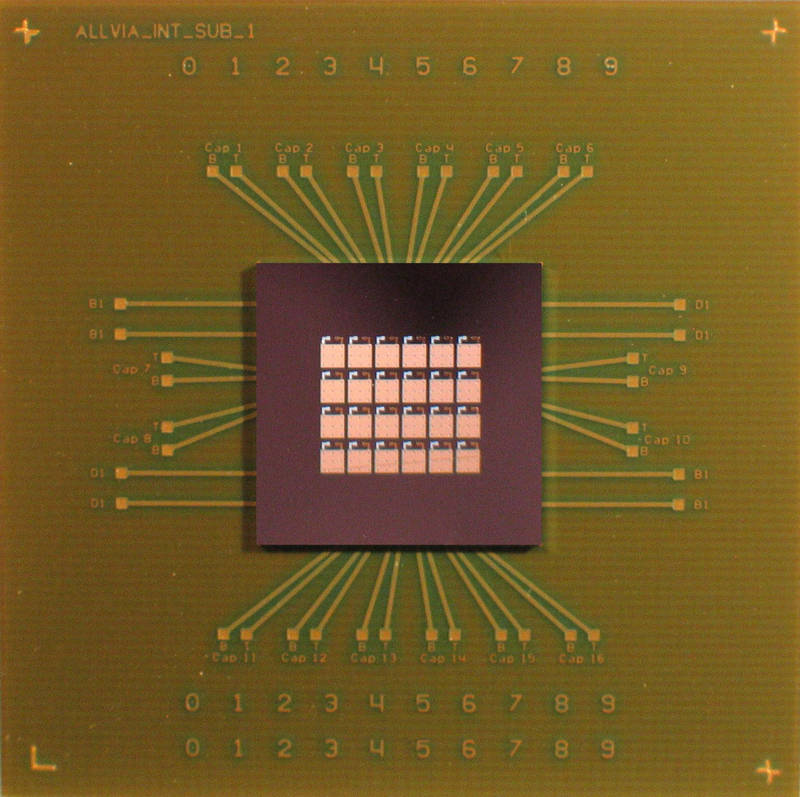
ALLVIA TSVs Help Integrate Passive Elements Directly Onto the Silicon Substrate in Much Higher Densities
| Source: ALLVIA
SUNNYVALE, CA--(Marketwire - February 23, 2010) - ALLVIA, the first through-silicon via (TSV)
foundry, has integrated embedded capacitors on Silicon Interposers, a key
interface between a silicon device and an organic substrate needed for
managing high interconnect densities. Capacitance values higher than 1,500
nF/cm2 have been achieved for the embedded capacitors developed for
delivering power to the devices. 3D integration with ALLVIA's
through-silicon via technology allows much closer access to high value
capacitors than previously possible, leading to a much higher level of
electrical performance.
Thin film capacitors
Thin film capacitors without TSVs have been used previously. However, with
the interconnect inductance being high, benefits of thin film capacitors
have not been fully realized. TSV interposers with embedded capacitors
provide the shortest electrical path between devices and power supply
decoupling capacitors. TSVs with their very low inductance interconnects
thus will enable very high electrical performance when integrated with
embedded thin film capacitors.
ALLVIA's silicon TSV interposers enable interconnect pitch matching between
a high-density IC chip and an organic or a ceramic substrate. Further,
they provide a very low stress interconnect to Si ICs that use low-k
dielectrics. These benefits make ALLVIA's interposers an attractive
solution for advanced packaging of next generation logic devices.
"The capacitance value of 15 nanofarads per millimeter square is not a
limit of our process and we think that the integration of capacitors with
TSVs and silicon interposers is a technological breakthrough. The
capacitance from the die or package can now be transferred to the
interposer," commented Sergey Savastiouk, CEO of ALLVIA.
Silicon Interposers
In January, ALLVIA announced that it had completed the integration of a
silicon interposer between a semiconductor die and an organic or ceramic
substrate and had completed reliability testing. This 3D integration of
substrates is made possible with ALLVIA's through-silicon vias. Samples and
reliability data are being made available to interested customers.
About ALLVIA
Located in Silicon Valley, ALLVIA is the first through-silicon via (TSV)
foundry and introduced the term "through-silicon via" in both a 1997
business plan and a January 2000 technical article. With the full spectrum
of facilities, IP and equipment, ALLVIA offers services for prototyping and
full volume production of both front side and back side TSVs to the MEMS
and semiconductor industries as well as silicon etching, copper plating,
photolithography, CMP, etc. www.allvia.com