TOKYO, JAPAN--(Marketwired - Jun 16, 2015) - Leading semiconductor test equipment supplier Advantest Corporation (
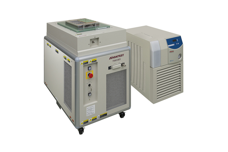
Amid surging sales of mobile electronics, DRAMs, NAND flash memories and multi-chip packages (MCPs) -- the main device types used in smart phones and tablets -- are quickly evolving toward higher speeds and greater device capacity. Internet and cloud servers also are driving demand for faster, higher-capacity ICs. Yet the cost of testing today's wide array of memory devices is an obstacle for chipmakers, which urgently require solutions that can deliver high functionality, high performance and low cost of test (COT). Advantest's new, multifunctional T5833 memory test system meets these needs, delivering both wafer sort and final test capabilities for a full range of memory devices, including LPDDR3-DRAMs, high-speed NAND flash memories and next-generation non-volatile memory ICs.
With a parallel test capacity of 2,048 devices for wafer test and 512 devices for final package test, the T5833 lowers costs by significantly reducing test time and boosting throughput. In addition to supporting known good die (KGD) testing at a maximum speed of 2.4 gigabits per second (Gbps), the T5833 also features a flexible site CPU architecture with multiple CPUs that enables optimized control of test processes.
The new system offers industry-leading capabilities in high-speed failure address storage and failure analysis, also known as memory redundancy. The speed of these two functions, both of which are indispensable for wafer sorting, reduces test time while enabling the recovery of more ICs for improved yield. In addition, both operations are scalable by making adjustments such as adding more CPUs for calculations.
Utilizing Advantest's AS modular memory test platform, the T5833 allows customers to choose the optimal system configuration for their needs, from engineering stations to large, volume-production systems. This extendibility allows the T5833 to handle future generations of devices and achieve higher throughput, which provides greater return on investment.
"Combining industry-best performance and low cost of test, the T5833 maximizes the efficiency of customers' investments," said Masuhiro Yamada, executive vice president, Memory Test Business Group at Advantest Corporation.
The T5833 tester joins the T5503HS system in Advantest's family of memory test systems, which has a worldwide installed base of more than 8,000 units, representing the company's leadership in the memory device test market.
About Advantest Corporation
A world-class technology company, Advantest is the leading producer of automatic test equipment (ATE) for the semiconductor industry and a premier manufacturer of measuring instruments used in the design and production of electronic instruments and systems. Its leading-edge systems and products are integrated into the most advanced semiconductor production lines in the world. The company also focuses on R&D for emerging markets that benefit from advancements in nanotech and terahertz technologies, and has introduced multi-vision metrology scanning electron microscopes essential to photomask manufacturing as well as groundbreaking 3D imaging and analysis tools. Founded in Tokyo in 1954, Advantest established its first subsidiary in 1982, in the USA, and now has subsidiaries worldwide. More information is available at www.advantest.com.
Contact Information:
Advantest Corporation
3061 Zanker Road
San Jose, CA 95134, USA
Judy Davies
VP of Global Marcom