Contact Information: Company Contact: ALLVIA, Inc. 657 N. Pastoria Ave. Sunnyvale, CA 94085 USA ph.: 408-720-3333 Agency Contact: Bruce Kirkpatrick 925.244.9100
Finally! A Semiconductor Technology Company Is Expanding; Through-Silicon Via Foundry, ALLVIA, Acquires Manufacturing Site in Oregon
Semiconductor Equipment Tool Selection Process to Begin Shortly; Benefits of Oregon Manufacturing Expansion Include Talent Pool and Lower Operating Costs
| Source: Allvia
SUNNYVALE, CA--(Marketwire - October 22, 2009) - ALLVIA, the first through-silicon via (TSV)
foundry, has purchased a manufacturing facility in Hillsboro, Oregon, for
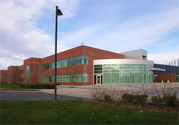
high volume production of their products with TSV technology. The former
semiconductor equipment manufacturing facility is a 178,000 square foot
building with 60,000 square feet of cleanroom capacity. The cleanroom is
expandable to 80,000 square feet.
Over the next several months ALLVIA will proceed with manufacturing
equipment tool selection for through-silicon via production. They expect
the facility to be operational in 2010 but no specific opening date has yet
been established.
Currently ALLVIA manufactures in Sunnyvale, CA, offering TSV prototyping
and volume production. The company will keep both facilities operational
for the foreseeable future and gradually move full volume production to the
Silicon Forest region of northwest Oregon as that facility builds out and
ramps up.
"In addition to the attractive purchase price of the building," commented
Sergey Savastiouk, CEO of ALLVIA, "there is a tremendous talent pool of
engineers and fab personnel in that community of Oregon. And operating
expenses, particularly electricity and water, but also including taxes, are
much more affordable compared to Silicon Valley."
Through-silicon vias
ALLVIA offers services for
both front side and back side TSVs and a full spectrum of facilities, IP
and equipment. They recently announced they had secured a next round of funding, bringing the
total invested in the company to $25 million. A portion of the new funds
was used to purchase the Oregon facility.
About ALLVIA
Located in Silicon Valley, ALLVIA is the first through-silicon via (TSV)
foundry and introduced the term "through-silicon via" in both a 1997
business plan and a January 2000 technical article. With the full spectrum
of facilities, IP and equipment, ALLVIA offers services for prototyping and
full volume production of both front side and back side TSVs to the MEMS
and semiconductor industries as well as silicon etching, copper plating,
photolithography, and CMP. www.allvia.com