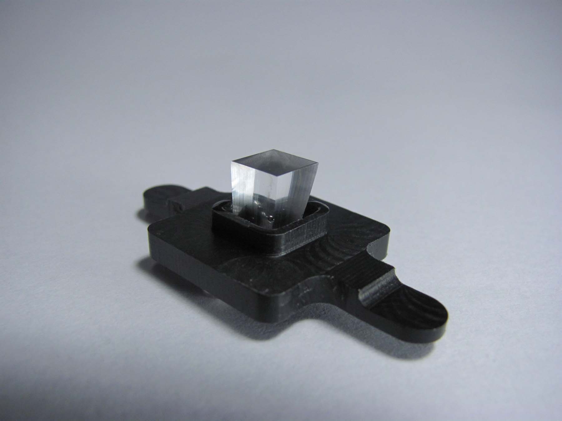
CHICAGO, IL--(Marketwire - May 1, 2012) - NanoInk announced today the availability of High Density (HD) Tip Arrays for Polymer Pen Lithography (PPL). These high-density elastomeric pen arrays are ideal for high-throughput deposition of ink materials. Similar to standard Dip Pen Nanolithography® (DPN®) with regular silicon nitride pens, High Density Tip Arrays can be used for the deposition of molecules with well-controlled feature size.
High Density Tip Arrays used for Polymer Pen Lithography can easily accommodate several thousands to millions of pens in the same array and are available in a range of array sizes (from 5x5 to 25x25 mm2) with different pen-to-pen pitches (from several microns to hundreds of microns pitch). The versatility of these arrays enables different types of applications in the fields of cell engineering, drug discovery, genomics and materials science.
"When integrated with the 2D leveling mechanism and the large range stage translation of the NLP 2000 System, the HD Tip Array becomes an extremely powerful tool for large scale and high throughput deposition," said Tom Warwick, general manager of NanoInk's NanoFabrication Systems Division. "With the release of HD Tip Array for PPL, we have enhanced our robust scalable nanofabrication offerings, following the earlier release of the NLP 2000 System in 2009 and 1 and 2D leveling in 2011."
NanoInk has devised a proprietary technique for the reliable fabrication of ultra-flat HD Tip Arrays, which can be customized around customer's application requirements. A recent video demonstrating the capability of HD Tip Arrays for PPL is available on NanoInkTV on YouTube. For inquiries about NanoInk's HD Tip Array offerings and customization, please contact Tom Warwick at NanoInk at (847)679-8807 or at sales@nanoink.net.
About NanoInk
NanoInk, Inc. is an emerging growth technology company specializing in nanometer-scale manufacturing and applications development for the life sciences, engineering, pharmaceutical, and education industries. Using Dip Pen Nanolithography® (DPN®) patented and proprietary nanofabrication technology, scientists are enabled to rapidly and easily create micro-and nanoscale structures from a variety of materials on a range of substrates. This low cost, easy to use and scalable technique brings sophisticated nanofabrication to the laboratory desktop. Headquartered in the Illinois Science + Technology Park, north of Chicago, NanoInk currently has several divisions including the NanoFabrication Systems Division, the Nano BioDiscovery Division, the NanoProfessor® Division and the NanoGuardian™ Division. For more information on products and services offered by NanoInk, Inc., visit www.nanoink.net.
NanoInk, the NanoInk logo, Dip Pen Nanolithography, and DPN are registered trademarks of NanoInk, Inc.
Contact Information:
Contacts:
Joshua Taustein
Dresner Corporate Services
(312)780-7219
jtaustein@dresnerco.com
David Gutierrez
Dresner Corporate Services
(312)780-7204
dgutierrez@dresnerco.com