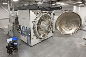
SAN JOSE, CA--(Marketwire - Mar 13, 2012) - Twin Creeks Technologies (www.twincreekstechnologies.com), a pioneer in next-generation manufacturing equipment for solar and semiconductor makers, today announced Hyperion: a wafer production system that dramatically reduces the cost of solar modules and semiconductor devices by reducing the amount of silicon and other substrate materials by up to 90 percent.
The key to Hyperion is thinness. Taking advantage of a technology called Proton Induced Exfoliation (PIE), Hyperion generates monocrystalline wafers that are less than 1/10th the thickness of conventional wafers. With thin wafers, manufacturers can profitably produce solar cells and other devices well below today's best-in-class cost structure. Twin Creeks estimates that Hyperion will permit manufacturers to produce solar cells for under 40 cents a watt in commercial-scale volume production facilities with prices declining over time.
Hyperion 3, the third-generation wafer production system designed and built by Twin Creeks, is the company's first commercial offering. It is available for shipment now.
"The thickness of wafers today is based on wafer slicing capabilities and the handling requirements for device processing. In reality, only the very top layer of a substrate plays an active role in generating energy or transmitting signals -- the rest is wasted," said Dr. Siva Sivaram, CEO of Twin Creeks. "By eliminating excess material, we will help solar manufacturers produce modules that compete with grid power and open up new markets for chip makers."
With PIE, Hyperion effectively uses atoms as a scalpel. Hyperion embeds a uniform layer of high-energy protons, which are hydrogen ions, into monocrystalline wafers to a depth of up to 20 microns. When heated, this new layer expands, cleaving the top surface from the donor wafer to form an ultra-thin wafer that is otherwise identical to the original. The ultra-thin wafer is then further processed into solar modules or semiconductors. Creating wafers with PIE also eliminates the kerf, or wasted silicon, in solar manufacturing.
Hyperion is compatible with a wide variety of monocrystalline wafers -- including germanium (used to make concentrated PV solar modules), gallium nitride, sapphire and silicon carbide (LEDs and power electronics). Twin Creeks has initially concentrated on helping manufacturers of crystalline silicon solar cells because of the urgent need to cut the cost of solar power. The lessons learned will further allow manufacturers to employ Hyperion for other applications, such as CMOS sensors.
By reducing the amount of silicon required in solar modules by 90 percent, Hyperion makes the entire silicon wafer value chain more efficient and dramatically lowers the capital needs of its customers. Manufacturers don't need as many saws, furnaces and crystal pullers to make the same amount of wafers.
Hyperion improves the monocrystalline silicon value proposition in other ways as well. In addition to being much lighter than conventional solar cells, cells produced with Hyperion wafers are also bendable, allowing manufacturers to consider flexible packaging and encapsulants for modules instead of glass. Additional layers of photovoltaic material can be added to wafers as well: Twin Creeks has produced heterojunction solar cells, which combine crystalline and amorphous silicon, in its development center. Over time, the combination of lower cost and lighter packaging will allow Twin Creeks customers to expand into other markets such as building-integrated photovoltaics (BIPV) and consumer electronics.
In keeping with providing a true manufacturing solution, Twin Creeks has developed intellectual property for creating and handling ultra-thin wafers as well as producing finished solar cells. This intellectual property can be licensed to Twin Creeks customers.
The company, in collaboration with the state of Mississippi, has built a commercial demonstration plant in Senatobia, Mississippi where Twin Creeks and its customers can fine-tune processes for generating ultra-thin solar modules and wafers with Hyperion. Senatobia is currently capable of producing 25 megawatts of solar cells a year and will be expanded to 100 megawatts. The company has obtained UL and TUV certification for heterojunction technology-based panels made at its Senatobia facility.
For more information, please visit our web site (www.twincreekstechnologies.com).
About Twin Creeks Technologies
Founded in 2008, Twin Creeks Technologies (www.twincreekstechnologies.com) is a leader in manufacturing equipment for thin crystalline wafers for the solar and semiconductor industries. The company's Hyperion 3 system, available now, produces wafers that are 90 percent thinner than conventional wafers and substantially reduce the cost of solar cells, power electronics semiconductors and other components. The company maintains R&D facilities in San Jose and Boston and is building a commercial-scale demonstration plant in Senatobia, Mississippi. It will also build facilities in Malaysia through a joint venture. Twin Creeks is backed by top-tier venture capital firms and loans and grants from the Mississippi Development Authority. Visit us on Twitter (https://twitter.com/#!/twincreekstech) and Facebook (http://facebook.com/twincreekstechnologies).
Contact Information:
For more information please contact:
Michael Kanellos
Eastwick Communications
(415) 820-4176
Kanellos@eastwick.com
